模拟开关、多路复用器、多路分解器
共 50+ 条- 匹配型号50+
- 有数据手册(前 50 条中)45
- 涉及品牌(前 50 条中)10
产品搜索结果共 50+ 条
| 对比 | 产品型号 | 品牌 | 分类 | 产品描述 | 技术资料 | 替代 | 操作 |
|---|---|---|---|---|---|---|---|
| 模拟开关、多路复用器、多路分解器 | 通道:2 类型:1:2 带宽:400MHz 导通电阻(Ω):4 | 查看详情 | |||||
| 模拟开关、多路复用器、多路分解器 | 通道:2 类型:1:2 带宽:30MHz 导通电阻(Ω):0.6 | 查看详情 | |||||
| 模拟开关、多路复用器、多路分解器 | MAX4645/MAX4646单刀单掷(SPST)模拟开关采用+5V电源供电时,导通电阻(RON)为2.5Ω(典型值)。RON在指定的信号范围内保持平坦(最大0.4Ω)。每个开关均可处理轨到轨模拟信号。+25°C时,最大关断漏电流为0.25nA。这些模拟开关非常适合低失真应用,在自动测试设备或需要电流切换的应用中优于机械继电器。它们的功率要求低,需要的电路板空间更少,并且比机械继电器更可靠。 这些开关采用+1.8V至+5V单电源供电,非常适合电池供电应用。MAX4645/MAX4646具有快速开关速度,开启时间(tON)为12ns,关断时间(tOFF)为8ns。 MAX4645为常开(NO)开关,MAX4646为常闭(NC)开关。两款器件均采用5引脚SOT23、6引脚SOT23和8引脚µMAX®封装。 | 查看详情 | |||||
| 模拟开关、多路复用器、多路分解器 | 通道:1 类型:1:1 带宽:300MHz 导通电阻(Ω):4.5 | 查看详情 | |||||
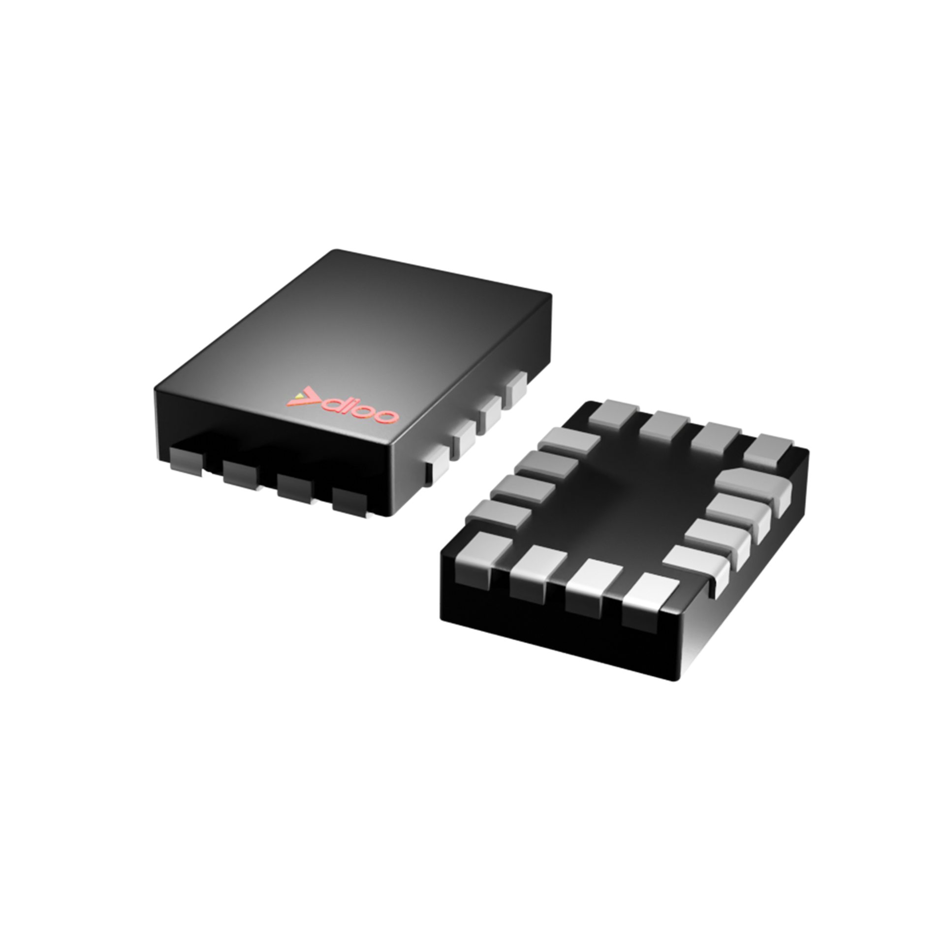
| 模拟开关、多路复用器、多路分解器 | The DIO1568 is a quad single-pole, double-throw (SPDT) analog switch targeted at dual SIM card multiplexing. The DIO1568 operates from a single 1.65 V to 5.5 V supply and features an ultra-low on-resistance of 0.85 Ω at SIM path to ensure minimal voltage drop in other paths. This device is fabricated with sub-micron CMOS technology to achieve fast switching speeds and is designed for break-before-make operation. The DIO1568 features a very low quiescent current even when the control voltage is lower than the VCC supply. This allows mobile handset applications direct interface with the baseband processor general-purpose I/Os. The DIO1568 provides two Green packages: QFN1.8*2.6-16 and QFN3*3-16. | 数据手册1 | 查看详情 | ||||
| 模拟开关、多路复用器、多路分解器 | 10 Ohm single-pole double-throw analog switch | 数据手册9 | 查看详情 | ||||
| 模拟开关、多路复用器、多路分解器 | 8-CH High-Performance CMOS Analog Multiplexer | 数据手册1 | 查看详情 | ||||
| 模拟开关、多路复用器、多路分解器 | CMOS Analog Multiplexer | 数据手册1 | 查看详情 | ||||
| 模拟开关、多路复用器、多路分解器 | High Isolation and Low Leakage 4:1 CMOS Analog Signal Multiplexer | 数据手册1 | 查看详情 | ||||
| 模拟开关、多路复用器、多路分解器 | 8:1 CMOS Analog Signal Multiplexer | 数据手册2 | 查看详情 | ||||
| 模拟开关、多路复用器、多路分解器 | Dual Bilateral Analog Switch | 数据手册2 | 查看详情 | ||||
| 模拟开关、多路复用器、多路分解器 | SPDT 1Ω Analog Switch | 数据手册1 | 查看详情 | ||||
| 模拟开关、多路复用器、多路分解器 | 3.5Ω, Low Voltage SPDT Analog Switch in Ultra-Thin Package | 数据手册2 | 查看详情 | ||||
| 模拟开关、多路复用器、多路分解器 | CMOS Analog Switch | 数据手册1 | 查看详情 | ||||
| 模拟开关、多路复用器、多路分解器 | Quad SPST CMOS Analog Switch | 数据手册1 | 查看详情 | ||||
| 模拟开关、多路复用器、多路分解器 | TPW3125 is high performance Single Pole/Double Throw (SPDT) analog switches. The devices feature ultra low R ON of 6Ω maximum at 4.5V V CC and will operate over the wide V CC range of 1.65V to 5.5V. The TPW3125 features very low quiescent current even when the control voltage is lower than the V CC supply. This feature services the portable applications very well allowing for the direct interface with processor general purpose I/Os, can tolerate 1.8V CMOS logic in select input when V CC supply is in the range of 4.75V to 5.25V. Status Production Rating Industrial Number of Channels 1 Switch Config 2:1 VCC (Min) (V) 1.65 VCC (Max) (V) 5.5 Input Range 0V to VCC BW (MHz) 250 IQ (μA) 0.3 Ron (Ω) 5 Leakage Current (nA) 10 VIH (Min) (V) 1.42 VIL (Max) (V) 0.7 tON (ns) 100 tOFF (ns) 100 Package SOT363 | 数据手册2 | 查看详情 | ||||
| 模拟开关、多路复用器、多路分解器 | Maxim's MAX312/MAX313/MAX314 analog switches feature low on-resistance (10Ω max) and 1.5Ω on-resistance matching between channels. These switches conduct equally well in either direction. They offer low leakage over temperature (2.5nA at +85°C). Low power consumption and ESD tolerance greater than 2000V per Method 3015.7 are guaranteed. The MAX312/MAX313/MAX314 are quad, single-pole/single-throw (SPST) analog switches. The MAX312 is normally closed (NC), and the MAX313 is normally open (NO). The MAX314 has two NC switches and two NO switches. All three devices operate from a single supply of +4.5V to +30V or from dual supplies of ±4.5V to ±20V. Applications Audio-Signal Routing Avionics Communication Systems Data Acquisition PBX/PABX Systems Sample-and-Hold Circuits Test Equipment | 数据手册5 | 查看详情 | ||||
| 模拟开关、多路复用器、多路分解器 | The TMUXHS221 is a high-speed bidirectional 2:1/1:2 multiplexer/demultiplexer optimized for USB 2.0 and eUSB2 LS, FS, and HS signaling. The TMUXHS221 is an analog passive switch that works for many high-speed interfaces for data rates up to 3 Gbps. The TMUXHS221 supports either differential or single ended CMOS signaling with a voltage range of −0.3 to 3.6 V. The excellent high speed performance of the TMUXHS221 results in minimal attenuation to the USB 2.0 or eUSB2 HS signal eye diagrams with very low channel ON resistance, high bandwidth, low reflection, and low added jitter. The device is optimized for excellent high frequency response so that passing USB 2.0 HS electrical compliance becomes easier. The datapaths of the device are also matched for best intra-pair skew performance. The TMUXHS221 has an extended temperature range that suits many rugged applications including industrial and high reliability use cases. . | 数据手册3 | 查看详情 | ||||
| 模拟开关、多路复用器、多路分解器 | The TMUX1247 is a general purpose complementary metal-oxide semiconductor (CMOS) single-pole double-throw (SPDT) switch. The TMUX1247 switches between two source inputs based on the state of the SEL pin. Wide operating supply of 1.08 V to 5.5 V allows for use in a broad array of applications from personal electronics to building automation. The device supports bidirectional analog and digital signals on the source (Sx) and drain (D) pins ranging from GND to V DD . A low supply current of 4 nA enables use in portable applications. All logic inputs have 1.8 V logic compatible thresholds, ensuring both TTL and CMOS logic compatibility when operating in the valid supply voltage range. Fail-Safe Logic circuitry allows voltages on the control pins to be applied before the supply pin, protecting the device from potential damage. | 数据手册3 | 查看详情 | ||||
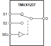
| 模拟开关、多路复用器、多路分解器 | The TMUX1237 is a general purpose 2:1, single-pole double-throw (SPDT), switch that supports a wide operating range of 1.08 V to 5.5 V. The device supports bidirectional analog and digital signals on the source (Sx) and drain (D) pins ranging from GND to V DD . The state of the select pin (SEL) controls which of the two sources pins are connected to the drain pin. Additionally, the TMUX1237 has a low supply current of 7 nA which enables the device to be used in a host of handheld or low power applications. The TMUX1237 improves system reliability by eliminating overshoot that might occur in a system due to switching between two voltage levels on the source (Sx) pins. In addition, the TMUX1237 also maintains fast switching times, enabling it to improve system performance for a wide range of applications from communications equipment to building automation. All logic inputs have 1.8 V logic compatible thresholds, ensuring both TTL and CMOS logic compatibility when operating in the valid supply voltage range. Fail-Safe Logic circuitry allows voltages on the control pins to be applied before the supply pin, protecting the device from potential damage. | 数据手册3 | 查看详情 |


申请芯片样品
填写型号和样品需求,供样安排确认后会联系你。