仪表放大器、运算放大器、缓冲放大器
共 50+ 条- 匹配型号50+
- 有数据手册(前 50 条中)47
- 涉及品牌(前 50 条中)4
产品搜索结果共 50+ 条
| 对比 | 产品型号 | 品牌 | 分类 | 产品描述 | 技术资料 | 替代 | 操作 |
|---|---|---|---|---|---|---|---|
| 仪表放大器、运算放大器、缓冲放大器 | The ADA4853-1/ADA4853-2/ADA4853-3 are low power, low cost, high speed, rail-to-rail output op amps with ultralow power disables that are ideal for portable consumer electronics. Despite their low price, the ADA4853-1/ADA4853-2/ADA4853-3 provide excellent overall performance and versatility. The 100 MHz, −3 dB bandwidth, and 120 V/μs slew rate make these amplifiers well-suited for many general-purpose, high speed applications. The ADA4853-1/ADA4853-2/ADA4853-3 voltage feedback op amps are designed to operate at supply voltages as low as 2.65 V and up to 5 V using only 1.4 mA of supply current per amplifier. To further reduce power consumption, the amplifiers are equipped with a power-down mode that lowers the supply current to less than 1.5 μA maximum, making them ideal in battery-powered applications. The ADA4853-1/ADA4853-2/ADA4853-3 provide users with a true single-supply capability, allowing input signals to extend 200 mV below the negative rail and to within 1.2 V of the positive rail. On the output, the amplifiers can swing within 200 mV of either supply rail. With their combination of low price, excellent differential gain (0.2%), differential phase (0.10°), and 0.5 dB flatness out to 22 MHz, these amplifiers are ideal for video applications. The ADA4853-1 is available in a 6-lead SC70, the ADA4853-2 is available in a 16-lead LFCSP_WQ, and the ADA4853-3 is available in both a 16-lead LFCSP_WQ and a 14-lead TSSOP. The ADA4853-1 temperature range is −40°C to +85°C while the ADA4853-2/ADA4853-3 temperature range is −40°C to +105°C. Applications Automotive infotainment systems Automotive safety systems Portable multimedia players Video cameras Digital still cameras Consumer video Clock buffer | 数据手册2 | 查看详情 | ||||
| 仪表放大器、运算放大器、缓冲放大器 | The OP200 is the first monolithic dual operational amplifier to offer OP77 type precision performance. Available in the industry standard 8-lead pinout, the OP200 combines precision performance with the space and cost savings offered by a dual amplifier. The OP200 features an extremely low input offset voltage of less than 75 μV with a drift below 0.5 μV/°C, guaranteed over the full military temperature range. Open-loop gain of the OP200 exceeds 5,000,000 into a 10 kΩ load; input bias current is under 2 nA; CMRR is over 120 dB; and PSRR is below 1.8 μV/V. On-chip Zener zap trimming is used to achieve the extremely low input offset voltage of the OP200 and eliminates the need for offset pulling. Power consumption of the OP200 is low, with each amplifier drawing less than 725 μA of supply current. The total current drawn by the dual OP200 is less than one-half that of a single OP07, yet the OP200 offers significant improvements over this industry-standard op amp. The voltage noise density of the OP200, 11 nV/√Hz at 1 kHz, is half that of most competitive devices. The OP200 is an ideal choice for applications requiring multiple precision op amps and where low power consumption is critical. For a quad precision op amp, see the OP400 . | 数据手册5 | 查看详情 | ||||
| 仪表放大器、运算放大器、缓冲放大器 | The OP292/OP492 are low cost, general-purpose dual and quad operational amplifiers designed for single-supply applications and are ideal for 5 V systems. Fabricated on Analog Devices, Inc., CBCMOS process, the OP292/OP492 series has a PNP input stage that allows the input voltage range to include ground. A BiCMOS output stage enables the output to swing to ground while sinking current. The OP292/OP492 series is unity-gain stable and features an outstanding combination of speed and performance for single-or dual-supply operation. The OP292/OP492 provide a high slew rate, high bandwidth, with open-loop gain exceeding 40,000 and offset voltage under 0.8 mV (OP292) and 1 mV (OP492). With these combinations of features and low supply current, the OP292/OP492 series is an excellent choice for battery-operated applications. The OP292/OP492 series performance is specified for single- or dual-supply voltage operation over the extended industrial temperature range (−40°C to +125°C).(OP292) and SO-14. Applications Disk drives Mobile phones Servo controls Modems and fax machines Pagers Power supply monitors and controls Battery-operated instrumentation | 数据手册2 | 查看详情 | ||||
| 仪表放大器、运算放大器、缓冲放大器 | The single MAX4091, dual MAX4092, and quad MAX4094 operational amplifiers combine excellent DC accuracy with rail-to-rail operation at the input and output. Since the common-mode voltage extends from V CC to V EE , the devices can operate from either a single supply (2.7V to 6V) or split supplies (±1.35V to ±3V). Each op amp requires less than 130µA of supply current. Even with this low current, the op amps are capable of driving a 1kΩ load, and the input-referred voltage noise is only 12nV/√Hz. In addition, these op amps can drive loads in excess of 2000pF. The precision performance of the MAX4091/MAX4092/MAX4094 combined with their wide input and output dynamic range, low-voltage, single-supply operation, and very low supply current, make them an ideal choice for battery-operated equipment, industrial, and data acquisition and control applications. In addition, the MAX4091 is available in space-saving 5-pin SOT23, 8-pin µMAX®, and 8-pin SO packages. The MAX4092 is available in 8-pin µMAX and SO packages, and the MAX4094 is available in 14-pin TSSOP and 14-pin SO packages. Applications Battery-Powered Instruments Cellular Handsets Data Acquisition and Control Digital Cameras (DIGICAMs) Glucose Meters GPS Solutions IP Camera Low-Voltage Signal Conditioning MP3 and Portable Media Players Portable Equipment | 数据手册3 | 查看详情 | ||||
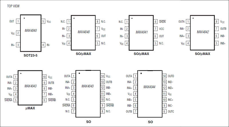
| 仪表放大器、运算放大器、缓冲放大器 | The MAX4040–MAX4044 family of micropower op amps operates from a single +2.4V to +5.5V supply or dual ±1.2V to ±2.75V supplies and have rail-to-rail input and output capabilities. These amplifiers provide a 90kHz gain-bandwidth product while using only 10µA of supply current per amplifier. The MAX4041/MAX4043 have a low-power shutdown mode that reduces supply current to less than 1µA and forces the output into a high-impedance state. The combination of low-voltage operation, rail-to-rail inputs and outputs, and ultra-low power consumption makes these devices ideal for any portable/battery-powered system. These amplifiers have outputs that typically swing to within 10mV of the rails with a 100kΩ load. Rail-to-rail input and output characteristics allow the full power-supply voltage to be used for signal range. The combination of low input offset voltage, low input bias current, and high open-loop gain makes them suitable for low-power/ low-voltage precision applications. The MAX4040 is offered in a space-saving 5-pin SOT23 package. All specifications are guaranteed over the -40°C to +85°C extended temperature range. Applications Battery Powered Systems Cellular Handsets Cellular Phones Digital Cameras (DIGICAMs) Digital Scales GPS Solutions MP3 and Portable Media Players Notebook Computers PDAs Portable/Battery-Powered Electronic Equipment Sensor Amplifiers Strain Gauges | 数据手册4 | 查看详情 | ||||
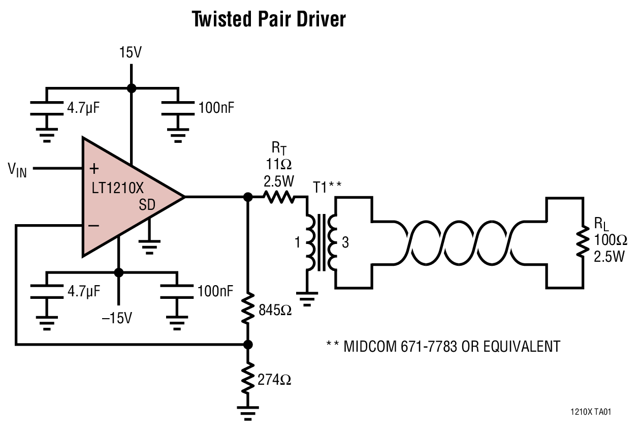
| 仪表放大器、运算放大器、缓冲放大器 | The LT1210X is a current feedback amplifier with high output current and excellent large-signal characteristics. The combination of high slew rate, 1.0A output drive and ±15V operation enables the device to deliver significant power at frequencies in the 1MHz to 2MHz range. Shortcircuit protection ensures the device’s ruggedness. The LT1210X is stable with large capacitive loads, and can easily supply the large currents required by the capacitive loading. A shutdown feature switches the device into a high impedance and low supply current mode, reducing dissipation when the device is not in use. For lower bandwidth applications, the supply current can be reduced with a single external resistor. The LT1210X is a member of a growing series of high temperature qualified products offered by Analog Devices. The LT1210X is available in the thermally enhanced TSSOP16-E package for operation with supplies from ±5V up to ±15V. The LT1210X is also available as dice. Applications Down-Hole Drilling and Instrumentation Heavy Industrial Avionics High Temperature Environments Cable Drivers Buffers Test Equipment Amplifiers Video Amplifiers ADSL Drivers | 数据手册3 | 查看详情 | ||||
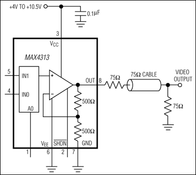
| 仪表放大器、运算放大器、缓冲放大器 | The MAX4310–MAX4315 single-supply mux-amps combine high-speed operation, low-glitch switching, and excellent video specifications. The six products in this family are differentiated by the number of multiplexer inputs and the gain configuration. The MAX4310/MAX4311/MAX4312 integrate 2-/4-/8-channel multiplexers, respectively, with an adjustable gain amplifier optimized for unity-gain stability. The MAX4313/MAX4314/MAX4315 integrate 2-/4-/8-channel multiplexers, respectively, with a +2V/V fixed-gain amplifier. All devices have 40ns channel switching time and low 10mVp-p switching transients, making them ideal for video-switching applications. They operate from a single +4V to +10.5V supply, or from dual supplies of ±2V to ±5.25V, and they feature Rail-to-Rail outputs and an input common-mode voltage range that extends to the negative supply rail. The MAX4310/MAX4311/MAX4312 have a -3dB bandwidth of 280MHz/345MHz/265MHz and up to a 460V/µs slew rate. The MAX4313/MAX4314/MAX4315, with 150MHz/127MHz/97MHz -3dB bandwidths up to a 540V/µs slew rate, and a fixed gain of +2V/V, are ideally suited for driving back-terminated cables. Quiescent supply current is as low as 6.1mA, while low-power shutdown mode reduces supply current to as low as 560µA and places the outputs in a high-impedance state. The MAX4310–MAX4315's internal amplifiers maintain an open-loop output impedance of only 8Ω over the full output voltage range, minimizing the gain error and bandwidth changes under loads typical of most rail-to-rail amplifiers. With differential gain and phase errors of 0.06% and 0.08°, respectively, these devices are ideal for broadcast video applications. Applications 75Ω Video Cable Drivers Broadcast Video Flash ADC Input Buffers High-Speed Signal Processing Medical Imaging Multimedia Products Video Crosspoint Switching Video Signal Multiplexing | 数据手册3 | 查看详情 | ||||
| 仪表放大器、运算放大器、缓冲放大器 | GS8141 — 聚洵 Gainsil 低压纳安级运算放大器 | 数据手册2 | 查看详情 | ||||
| 仪表放大器、运算放大器、缓冲放大器 | GS8554 — 聚洵 Gainsil 零漂移运算放大器 | 数据手册1 | 查看详情 | ||||
| 仪表放大器、运算放大器、缓冲放大器 | GS8332 — 聚洵 Gainsil 零漂移运算放大器 | 数据手册2 | 查看详情 | ||||
| 仪表放大器、运算放大器、缓冲放大器 | GS8331 — 聚洵 Gainsil 零漂移运算放大器 | 数据手册2 | 查看详情 | ||||
| 仪表放大器、运算放大器、缓冲放大器 | LTC8391/8392单通道与双通道运算放大器通过专有技术实现了输入失调电压校正,具备低失调(最大±120 µV)和低温漂(最大0.5 µV/℃)特性。该系列器件兼具轨到轨输入输出摆幅、低静态电流(5V供电下典型值为28 µA)、330kHz宽带宽以及极低噪声(0.1至10Hz频带内为2 μV峰峰值)等特点,使其在手机、平板电脑、笔记本电脑和便携式医疗设备等多种电池供电应用中极具吸引力。低输入偏置电流特性支持该系列放大器应用于具有兆欧级源阻抗的电路。 LTC8391/8392放大器非常适合需要对微弱信号进行精密放大、且不容许误差源存在的应用场景,即使是在需要高带宽和快速瞬态响应的条件下也是如此。轨到轨的输入输出摆幅使其易于实现高边和低边检测。该系列可在低至1.8V的单电源电压下工作,适用于两节电池供电的应用。 LTC8391/8392放大器增强了电磁干扰(EMI)保护功能,以最大限度地减少外部电磁干扰的影响,并具备高静电放电(ESD)保护能力(5kV HBM)。所有型号均适用于-40℃至+125℃的扩展工业温度范围。 | 数据手册1 | 查看详情 | ||||
| 仪表放大器、运算放大器、缓冲放大器 | 数据手册1 | 查看详情 | |||||
| 仪表放大器、运算放大器、缓冲放大器 | 数据手册1 | 查看详情 | |||||
| 仪表放大器、运算放大器、缓冲放大器 | 查看详情 | ||||||
| 仪表放大器、运算放大器、缓冲放大器 | 查看详情 | ||||||
| 仪表放大器、运算放大器、缓冲放大器 | 查看详情 | ||||||
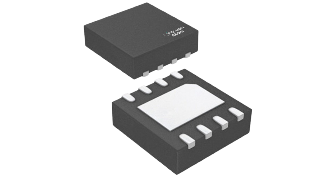
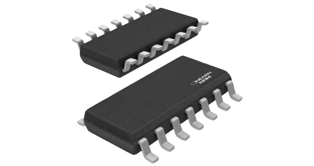
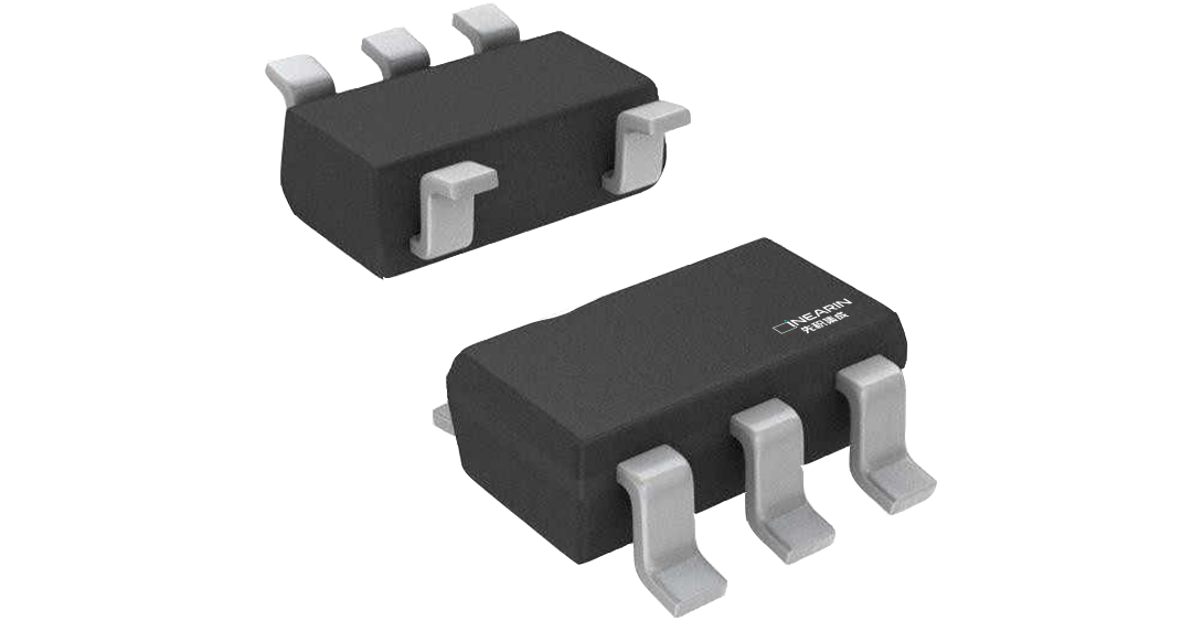
| 仪表放大器、运算放大器、缓冲放大器 | LTC881x系列单通道、双通道及四通道放大器最大化了增益带宽与电源电流的比值,非常适合便携式仪器、便携医疗设备、可穿戴健身设备和无线远程传感器等电池供电应用。该系列具备轨到轨输入输出摆幅、15 kHz带宽、超低电源电流(5.0 V供电下每放大器典型值600 nA)以及低噪声(0.1至10 Hz频带内6.3 μV峰峰值)特性,是精密、成本优化、"始终在线"型传感应用的出色选择。 LTC881x放大器的稳健设计为电路设计者提供了易用性:集成了射频/电磁干扰抑制滤波器,过驱条件下无相位反转,并具备高静电放电保护能力(5-kV HBM)。该系列放大器针对低至+1.7 V(±0.85 V)、高达+5.5 V(±2.75 V)的工作电压进行了优化,支持-40℃至+85℃的扩展温度范围。 LTC8811/3(单通道)提供SOT23-5L和SC70-5L封装。LTC8812(双通道)提供DFN-8L、SOIC-8L和MSOP-8L封装。四通道LTC8814提供QFN-16L、SOIC-14L和TSSOP-14L封装。 | 数据手册2 | 查看详情 | ||||
| 仪表放大器、运算放大器、缓冲放大器 | LTC882x系列单通道、双通道及四通道放大器最大化了增益带宽积与电源电流的比值,非常适合可穿戴设备、手机、平板电脑和便携式医疗设备等电池供电应用。该系列具备轨到轨输入输出摆幅、500 kHz宽带宽、超低电源电流(VS=5.5V供电下每放大器典型值6.6 µA)以及低噪声(0.1至10 Hz频带内6 μV峰峰值)特性,是精密或通用型、低电流、低压、电池供电应用的出色选择。低输入偏置电流支持这些放大器应用于具有兆欧级源阻抗的场景。 LTC882x运算放大器的稳健设计为电路设计者提供了易用性:集成了射频/电磁干扰抑制滤波器,过驱条件下无相位反转,并具备高静电放电保护能力(5-kV HBM)。该系列放大器针对低至+1.8 V(±0.9 V)、高达+5.5 V(±2.75 V)的工作电压进行了优化。 LTC8821(单通道)提供SOT23-5L和SC70-5L封装。LTC8822(双通道)提供DFN-8L、SOIC-8L和MSOP-8L封装。四通道LTC8824提供SOIC-14L和TSSOP-14L封装。所有器件均支持-40℃至+125℃的扩展温度范围。 | 数据手册1 | 查看详情 | ||||
| 仪表放大器、运算放大器、缓冲放大器 | LTC881x系列单通道、双通道及四通道放大器最大化了增益带宽与电源电流的比值,非常适合便携式仪器、便携医疗设备、可穿戴健身设备和无线远程传感器等电池供电应用。该系列具备轨到轨输入输出摆幅、15 kHz带宽、超低电源电流(5.0 V供电下每放大器典型值600 nA)以及低噪声(0.1至10 Hz频带内6.3 μV峰峰值)特性,是精密、成本优化、"始终在线"型传感应用的出色选择。 LTC881x放大器的稳健设计为电路设计者提供了易用性:集成了射频/电磁干扰抑制滤波器,过驱条件下无相位反转,并具备高静电放电保护能力(5-kV HBM)。该系列放大器针对低至+1.7 V(±0.85 V)、高达+5.5 V(±2.75 V)的工作电压进行了优化,支持-40℃至+85℃的扩展温度范围。 LTC8811/3(单通道)提供SOT23-5L和SC70-5L封装。LTC8812(双通道)提供DFN-8L、SOIC-8L和MSOP-8L封装。四通道LTC8814提供QFN-16L、SOIC-14L和TSSOP-14L封装。 | 数据手册2 | 查看详情 |






申请芯片样品
填写型号和样品需求,供样安排确认后会联系你。