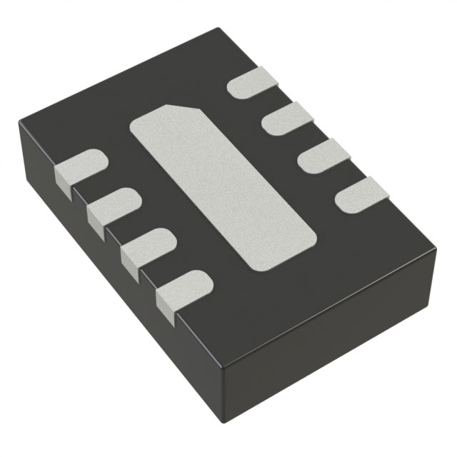
Analog Devices Inc.United States
IC RF DETECT 100MHZ-2.7GHZ 8CSP
AD8314ACPZ-RL7 is an RF detector/controller for 100 MHz to 2.7 GHz with a 45 dB dynamic range, in an 8-lead LFCSP package, operating from -40°C to +85°C, featuring low-power shutdown.Checked against the datasheet
All alternatives
View full reportTechnical parameters
Datasheet-verified parameters
26 items| Parameter | Value and test conditions | Source |
|---|---|---|
| Package | 8-Lead LFCSP, 7'' Tape and Reel (CP-8-23) | |
| Operating Temperature Range | -40°C to +85°C | |
| RoHS Compliant | Z = RoHS Compliant Part | |
| Frequency Range | 0.1 GHz to 2.5 GHz (To meet all specifications); 100 MHz to 2.7 GHz (General Description) | |
| Input Voltage Range | 1.25 mV rms to 224 mV rms (Internally ac-coupled) | |
| Equivalent Power Range | -45 dBm to 0 dBm (52.3 Ω external termination) |
All parameters (14)
| Power | |
|---|---|
| Current - Supply | 5.7 mA |
| Voltage - Supply | 2.7V ~ 5.5V |
| AC and DC characteristics | |
| Accuracy | - |
| Frequency | 100MHz ~ 2.7GHz |
| Environment and package | |
| Mounting Type | Surface Mount |
| Package | Tape & Reel (TR) Cut Tape (CT) Digi-Reel® |
| Package / Case | 8-VFDFN Exposed Pad, CSP |
| Supplier Device Package | 8-LFCSP-VD (3x2) |
| Other | |
| Base Product Number | AD8314 |
| Input Range | -45dBm ~ 0dBm |
| Mfr | Analog Devices Inc. |
| Product Status | Active |
| RF Type | Cellular, GSM, TDMA, CDMA |
| Series | - |
Pinout and package
Figure 3. CP-8-23 Pin Configur…
| Pin | Name | Function | Source |
|---|---|---|---|
| 1 | RF | Input | |
| 2 | Enable Control (Connect to VS for Normal Operation, Ground for Disable) | ||
| 3 | Setpoint Input for Controller Mode (Connect to V_UP for Detector Mode) | ||
| 4 | Filter Capacitor Connection (Between FLTR and V_UP) | ||
| 5 | Device Common (Ground) | ||
| 6 | Logarithmic Output (Voltage increases with input amplitude) | ||
| 7 | Inverted Output (V_DN = 2.25 V - 2 × V_UP) | ||
| 8 | Positive Supply Voltage (2.7 V to 5.5 V) | ||
| EPAD | Exposed Pad (Connect to ground via low impedance path) |
Documents
Datasheet-verified content is extracted by AI from the manufacturer datasheet. Click a page number to view the original.