Analog Devices Inc.United States
ADG749BKSZ-REEL
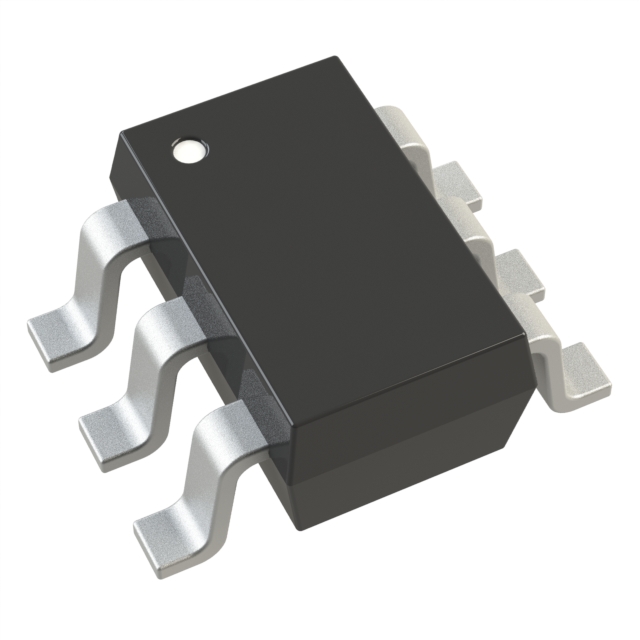
ActiveAnalog Switches, Multiplexers, Demultiplexers6-Lead Thin Shrink Small Outline Transistor Package [SC70]IC SWITCH SPDT X 1 5OHM SC70-6
ADG749BKSZ-REEL is a CMOS SPDT analog switch with 1.8V to 5.5V single supply, max 5Ω on-resistance, >200MHz -3dB bandwidth, 6-lead SC70 package, operating temperature -40°C to +125°C, and RoHS compliant.Checked against the datasheet
All alternatives
View full report7 alternatives on file, including 2 Chinese alternatives. Sign in to view them.
Technical parameters
Key specs
Switch circuitSPDT
Circuits1
On-resistance5 ΩMax
Supply voltage1.8 ~ 5.5 V
Datasheet-verified parameters
23 items| Parameter | Value and test conditions | Source |
|---|---|---|
| Switch Circuit | SPDT (Single Pole Double Throw) | |
| Number of Channels | 1 (SPDT) | |
| On Resistance | 5 Ω (maximum) at 5 V; 10 Ω (maximum) at 3 V; typically 40 Ω at 1.8 V | |
| Supply Voltage | 1.8 V to 5.5 V | |
| Package | 6-Lead Thin Shrink Small Outline Transistor Package [SC70] | |
| Operating Temperature Range | -40°C to +125°C |
All parameters (22)
| Power | |
|---|---|
| Channel Capacitance (CS(off), CD(off)) | 7pF |
| Channel-to-Channel Matching (ΔRon) | - |
| Current - Leakage (IS(off)) (Max) | 250pA |
| Voltage - Supply, Dual (V±) | - |
| Voltage - Supply, Single (V+) | 1.8V ~ 5.5V |
| AC and DC characteristics | |
| -3db Bandwidth | 200MHz |
| Environment and package | |
| Mounting Type | Surface Mount |
| Operating Temperature | -40°C ~ 125°C (TA) |
| Package | Tape & Reel (TR) Cut Tape (CT) Digi-Reel® |
| Package / Case | 6-TSSOP, SC-88, SOT-363 |
| Supplier Device Package | SC-70-6 |
| Other | |
| Base Product Number | ADG749 |
| Charge Injection | - |
| Crosstalk | -82dB @ 1MHz |
| Mfr | Analog Devices Inc. |
| Multiplexer/Demultiplexer Circuit | 2:1 |
| Number of Circuits | 1 |
| On-State Resistance (Max) | 5Ohm |
| Product Status | Active |
| Series | - |
| Switch Circuit | SPDT |
| Switch Time (Ton, Toff) (Max) | 7ns, 3ns (Typ) |
Pinout and package
Figure 2. Pin Configuration
| Pin | Name | Function | Source |
|---|---|---|---|
| 1 | IN: Digital control input pin | ||
| 2 | VDD: Most positive power supply pin | ||
| 3 | GND: Ground (0 V) reference pin | ||
| 4 | S1: Source terminal of the multiplexer. Can be used as input or output | ||
| 5 | D: Drain terminal of the multiplexer. Can be used as input or output | ||
| 6 | S2: Source terminal of the multiplexer. Can be used as input or output |
Documents
Datasheet-verified content is extracted by AI from the manufacturer datasheet. Click a page number to view the original.