Analog Devices Inc.United States
IC CLK DATA REC SDH 1.25GHZ
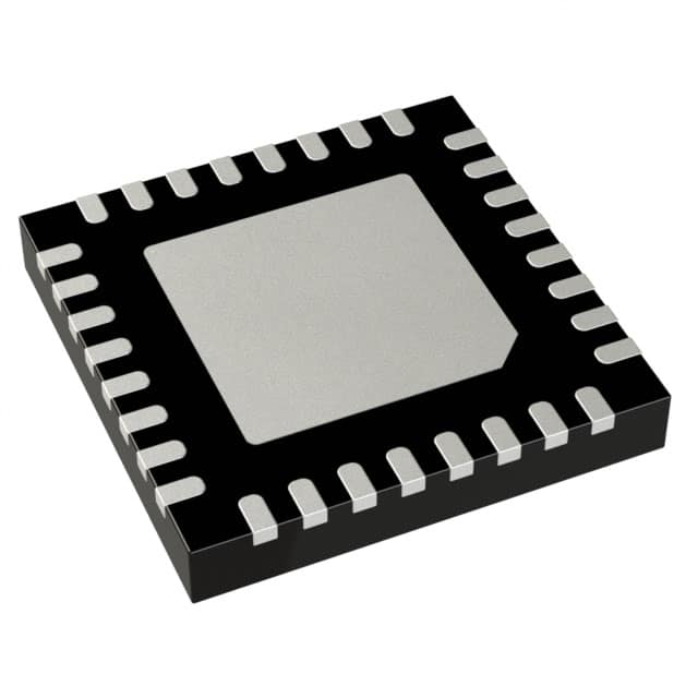
The ADN2813ACPZ-500RL7 is a 10 Mb/s to 1.25 Gb/s clock and data recovery IC with an integrated limiting amplifier, in a 32-lead LFCSP package, operating from -40°C to +85°C, with I2C interface.Checked against the datasheet
All alternatives
View full reportTechnical parameters
Datasheet-verified parameters
20 items| Parameter | Value and test conditions | Source |
|---|---|---|
| Package | 32-Lead LFCSP_WQ, 7'' Tape and Reel, 500 Pieces | |
| Operating Temperature Range | -40°C to +85°C | |
| RoHS | Compliant (Z = RoHS Compliant Part) | |
| Power Supply Voltage | Min: 3.0 V, Typ: 3.3 V, Max: 3.6 V | |
| Power Supply Current | Typ: 139 mA, Max: 155 mA (Locked to 1.25 Gb/s) | |
| Data Rate | Min: 10 Mb/s, Max: 1250 Mb/s |
All parameters (18)
| Power | |
|---|---|
| Voltage - Supply | 3V ~ 3.6V |
| AC and DC characteristics | |
| Frequency - Max | 1.25GHz |
| Environment and package | |
| Mounting Type | Surface Mount |
| Operating Temperature | -40°C~85°C |
| Package | Tape & Reel (TR); Cut Tape (CT); Digi-Reel® |
| Package / Case | 32-WFQFN Exposed Pad, CSP |
| Supplier Device Package | 32-LFCSP-WQ (5x5) |
| Other | |
| Base Product Number | ADN2813 |
| Differential - Input:Output | Yes/Yes |
| Input | CML |
| Main Purpose | SONET/SDH |
| Mfr | Analog Devices Inc. |
| Number of Circuits | 1 |
| Output | LVDS |
| PLL | Yes |
| Product Status | Active |
| Ratio - Input:Output | 1:2 |
| Series | - |
Pinout and package
\* THERE IS AN EXPOSED PAD ON …
| Pin | Name | Function | Source |
|---|---|---|---|
| 1 | VCC: Connect to VCC | ||
| 2 | VCC: Power for Limiting Amplifier, LOS | ||
| 3 | VREF: Internal VREF Voltage. Decouple to GND with a 0.1 μF capacitor | ||
| 4 | NIN: Differential Data Input. CML | ||
| 5 | PIN: Differential Data Input. CML | ||
| 6 | SLICEP: Differential Slice Level Adjust Input | ||
| 7 | SLICEN: Differential Slice Level Adjust Input | ||
| 8 | VEE: GND for Limiting Amplifier, LOS | ||
| 9 | THRADJ: LOS Threshold Setting Resistor | ||
| 10 | REFCLKP: Differential REFCLK Input. 10 MHz to 160 MHz | ||
| 11 | REFCLKN: Differential REFCLK Input. 10 MHz to 160 MHz | ||
| 12 | VCC: VCO Power | ||
| 13 | VEE: VCO GND | ||
| 14 | CF2: Frequency Loop Capacitor | ||
| 15 | CF1: Frequency Loop Capacitor | ||
| 16 | LOL: Loss-of-Lock Indicator. LVTTL active high | ||
| 17 | VEE: FLL Detector GND | ||
| 18 | VCC: FLL Detector Power | ||
| 19 | SADDR5: Slave Address Bit 5 | ||
| 20 | SCK: I2C Clock Input | ||
| 21 | SDA: I2C Data Input | ||
| 22 | LOS: Loss-of-Signal Detect Output. Active high. LVTTL | ||
| 23 | VEE: Output Buffer, I2C GND | ||
| 24 | VCC: Output Buffer, I2C Power | ||
| 25 | CLKOUTN: Differential Recovered Clock Output. LVDS | ||
| 26 | CLKOUTP: Differential Recovered Clock Output. LVDS | ||
| 27 | SQUELCH: Disable Clock and Data Outputs. Active high. LVTTL | ||
| 28 | DATAOUTN: Differential Recovered Data Output. LVDS | ||
| 29 | DATAOUTP: Differential Recovered Data Output. LVDS | ||
| 30 | VEE: Phase Detector, Phase Shifter GND | ||
| 31 | VCC: Phase Detector, Phase Shifter Power | ||
| 32 | VCC: Connect to VCC | ||
| Exposed Pad | Pad: Connect to GND. Works as a heat sink |
Documents
Datasheet-verified content is extracted by AI from the manufacturer datasheet. Click a page number to view the original.