FFE-PAGE-44
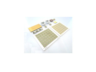
ActiveThick film printing is to print metal films such as conductor and resistive element on ceramic substrate which makes going into high-temperature baking process for finalization of composite module substrate. This thick film printing technology is applied to our products; resistor network, capacitor array, diode array, LED module and hybrid IC. * Thermal design is available by use of alumina substrate that is good for heat conduction. * Space-saving is achievable to make composite circuit. * Able to assign placement freely and can make any sizes of resistive element on the substrate. * Resistive element that is made by laser triming is guaranteed high accuracy and high reliability. * Available to consult about functional triming for resistive element that is to influence entire circuit function.
All alternatives
View full reportTechnical parameters
| Name | Thick film printing |
| Overview | Thick film printing is to print metal films such as conductor and resistive element on ceramic substrate which makes going into high-temperature baking process for finalization of composite module substrate. This thick film printing technology is applied to our products; resistor network, capacitor array, diode array, LED module and hybrid IC. * Thermal design is available by use of alumina substrate that is good for heat conduction. * Space-saving is achievable to make composite circuit. * Able to assign placement freely and can make any sizes of resistive element on the substrate. * Resistive element that is made by laser triming is guaranteed high accuracy and high reliability. * Available to consult about functional triming for resistive element that is to influence entire circuit function. |
Documents
No documents are linked to this part yet.