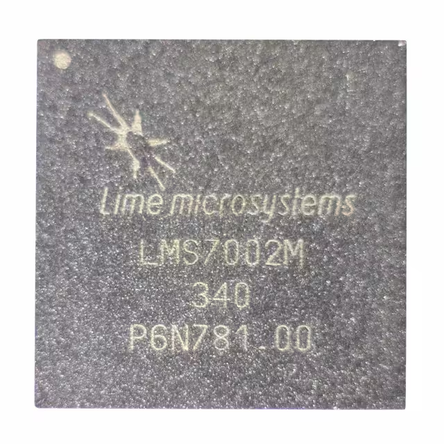
Lime Microsystems LtdUnited Kingdom
IC RF TXRX+MCU CELLULAR 261SMD
LMS7002M is a 100 kHz to 3.8 GHz FPRF MIMO transceiver IC with integrated microcontroller and 12-bit ADC/DAC, in a 261-pin aQFN package, supporting TDD/FDD and LimeLight interface.Checked against the datasheet
All alternatives
View full reportTechnical parameters
Datasheet-verified parameters
24 items| Parameter | Value and test conditions | Source |
|---|---|---|
| Package | 261 pin aQFN 11.5x11.5 mm | |
| Operating Temperature Range | Min: -40 °C, Typ: 25 °C, Max: 85 °C | |
| Storage Temperature Range | Min: -65 °C, Typ: 25 °C, Max: 125 °C | |
| Operating Frequency Range | Min: 300.1 MHz, Max: 3800 MHz (Extended by TSP NCOs) | |
| RF Modulation Bandwidth | Max: 48 MHz (Through digital interface MIMO), 96 MHz (Through digital interface SISO), 160 MHz (Through analog interface) | |
| Frequency Resolution | Max: 24.8 Hz (Using 52 MHz PLL reference clock) |
All parameters (20)
| Power | |
|---|---|
| Current - Receiving | 420mA |
| Current - Transmitting | 350mA |
| Power - Output | 0dBm |
| Voltage - Supply | 1.1V ~ 1.89V |
| AC and DC characteristics | |
| Frequency | 100kHz ~ 3.8GHz |
| Environment and package | |
| Memory Size | 10kB SRAM |
| Operating Temperature | -40°C~85°C |
| Package | Tray |
| Package / Case | 261-SMD Module |
| Other | |
| Base Product Number | LMS7002 |
| Data Rate (Max) | - |
| Mfr | Lime Microsystems Ltd |
| Modulation | - |
| Product Status | Active |
| Protocol | CDMA, GSM, HSPA, LTE, TD-SCDMA, WCDMA |
| RF Family/Standard | Cellular |
| Sensitivity | - |
| Serial Interfaces | SPI |
| Series | - |
| Type | TxRx + MCU |
Pinout and package
Package261 pin aQFN 11.5x11.5 mm
| Pin | Name | Function | Source |
|---|---|---|---|
| 1 | UNUSED | ||
| 5 | VDD12_TXBUF | (1.25V supply – TX XOSC buffer) | |
| 6 | VDD18_TXBUF | (1.8V supply – TX XOSC buffer) | |
| 8 | VDD18_VCO_SXT | (1.8V supply – TX SX VCO) | |
| 9 | VDD12O_VCO_SXT | (1.25V supply – TX SX VCO) | |
| 10 | VDD12_VCO_SXT | (1.25V supply – TX SX VCO) | |
| 12 | GND_VCO_SXT | (GND – TX SX VCO) | |
| 13 | VDD_CP_SXT | (1.25V supply – TX SX Charge pump) | |
| 14 | GND_CP_SXT | (GND – TX SX Charge pump) | |
| 15 | VDD_DIV_SXT | (1.25V supply – TX SX frequency divider) | |
| 17 | VDDO_DIV_SXT | (1.25V supply – TX SX frequency divider) | |
| 19 | GND_DIV_SXT | (GND – TX SX frequency divider) | |
| 20 | DVDD_SXT | (1.25V supply – digital supply for TX SX) | |
| 22 | DGND_SXT | (GND – digital supply for TX SX) | |
| 23 | VDD18_LDO_TX | (1.8V supply – TX LDO) | |
| 24 | VDD_TBB | (1.25V supply – TX baseband) | |
| 25 | tbbqn_pad_1 (in – TX change input pad to externally drive the TX BB Channel 1) | ||
| 26 | tbbin_pad_1 (in – TX change input pad to externally drive the TX BB Channel 1) | ||
| 27 | tbbqp_pad_1 (in – TX change input pad to externally drive the TX BB Channel 1) | ||
| 28 | tbbin_pad_2 (in – TX change input pad to externally drive the TX BB Channel 2) | ||
| 29 | tbbip_pad_1 (in – TX change input pad to externally drive the TX BB Channel 1) | ||
| 30 | adcin_in_1 (in – ADC input pads – To use external filtering Channel 1) | ||
| 31 | tbbqp_pad_2 (in – TX change input pad to externally drive the TX BB Channel 2) | ||
| 32 | tbbqn_pad_2 (in – TX change input pad to externally drive the TX BB Channel 2) | ||
| 33 | tbbip_pad_2 (in – TX change input pad to externally drive the TX BB Channel 2) | ||
| 34 | adcin_ip_1 (in – ADC input pads – To use external filtering Channel 1) | ||
| 35 | adcin_in_2 (in – ADC input pads – To use external filtering Channel 2) | ||
| 36 | adcin_qn_1 (in – ADC input pads – To use external filtering Channel 1) | ||
| 37 | adcin_qp_1 (in – ADC input pads – To use external filtering Channel 1) | ||
| 38 | adcin_qn_2 (in – ADC input pads – To use external filtering Channel 2) | ||
| 39 | adcin_ip_2 (in – ADC input pads – To use external filtering Channel 2) | ||
| 40 | rbbip_pad_1 (out – RX BB output – To use external filtering Channel 1) | ||
| 41 | adcin_qp_2 (in – ADC input pads – To use external filtering Channel 2) | ||
| 42 | rbbqn_pad_1 (out – RX BB output – To use external filtering Channel 1) | ||
| 43 | rbbin_pad_1 (out – RX BB output – To use external filtering Channel 1) | ||
| 44 | rbbqp_pad_1 (out – RX BB output – To use external filtering Channel 1) | ||
| 45 | rbbin_pad_2 (out – RX BB output – To use external filtering Channel 2) | ||
| 46 | rbbqn_pad_2 (out – RX BB output – To use external filtering Channel 2) | ||
| 47 | rbbip_pad_2 (out – RX BB output – To use external filtering Channel 2) | ||
| 48 | rbbqp_pad_2 (out – RX BB output – To use external filtering Channel 2) | ||
| 50 | VDD14_RBB | (1.4V supply- RX baseband) | |
| 51 | VDD18_TIA_RFE | (1.8V supply- RXFE TIA) | |
| 52 | VDD14_TIA_RFE | (1.4V supply- RXFE TIA) | |
| 53 | VDD12_TIA_RFE | (1.25V supply- RXFE TIA) | |
| 55 | VDD18_LDO_RX | (1.8V supply- RX LDO) | |
| 59 | VDD14_LNA_RFE | (1.4V supply- RXFE LNA) | |
| 60 | VDD12_LNA_RFE | (1.25V supply- RXFE LNA) | |
| 68 | rfgp_w_RFE_2 (in – LNA input gate Wideband LNA – Gate : Channel 2) | ||
| 69 | rfgn_w_RFE_2 (in – LNA input gate Wideband LNA – Gate : Channel 2) | ||
| 72 | rfsn_I_RFE_2 (in/out – LNA Lowband LNA – Source: Channel 2) | ||
| 73 | rfgp_I_RFE_2 (in – LNA input gate Lowband LNA – Gate : Channel 2) | ||
| 77 | rfsp_I_RFE_2 (in/out – LNA Lowband LNA – Source : Channel 2) | ||
| 78 | rfgn_I_RFE_2 (in – LNA input gate Lowband LNA – Gate : Channel 2) | ||
| 79 | rfgp_h_RFE_2 (in – LNA input gate Highband LNA – Gate : Channel 2) | ||
| 80 | rfgn_h_RFE_2 (in – LNA input gate Highband LNA – Gate : Channel 2) | ||
| 84 | rfgp_w_RFE_1 (in – LNA input gate Wideband LNA – Gate : Channel 1) | ||
| 87 | rfgn_w_RFE_1 (in – LNA input gate Wideband LNA – Gate : Channel 1) | ||
| 88 | rfsn_I_RFE_1 (in/out – LNA Lowband LNA – Source : Channel 1) | ||
| 89 | rfgp_I_RFE_1 (in – LNA input gate Lowband LNA – Gate : Channel 1) | ||
| 91 | rfgn_I_RFE_1 (in – LNA input gate Lowband LNA – Gate : Channel 1) | ||
| 92 | rfsp_I_RFE_1 (in/out – LNA Lowband LNA – Source : Channel 1) | ||
| 93 | rfgp_h_RFE_1 (in – LNA input gate Highband LNA – Gate : Channel 1) | ||
| 94 | rfgn_h_RFE_1 (in – LNA input gate Highband LNA – Gate : Channel 1) | ||
| 95 | VDD_MXLOBUF_RFE | (1.25V supply: RX LO buffers) |
Documents
Datasheet-verified content is extracted by AI from the manufacturer datasheet. Click a page number to view the original.