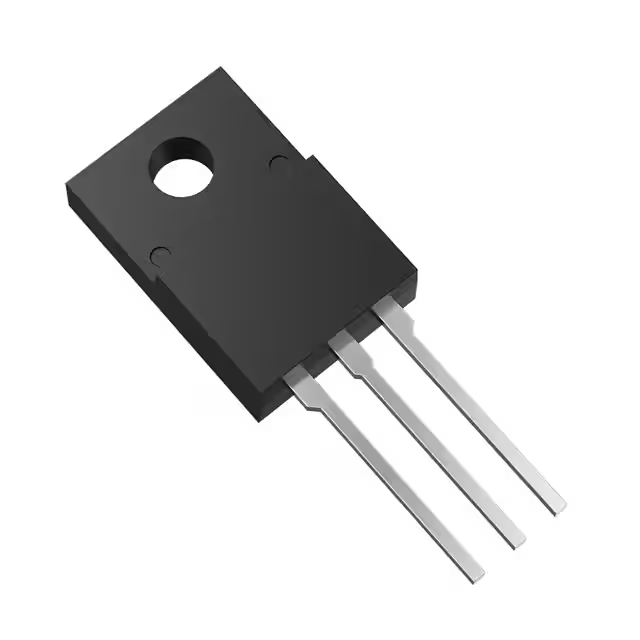
MOSFET N-CH 650V 11.1A TO220SIS
All alternatives
View full reportTechnical parameters
Key specs
ChannelN-channel
Drain-source voltage650 V
Continuous drain current11.1 A
On-resistance390 mΩMax · 5.5A
Gate threshold voltage3.5 VMax · 450μA
| Power | |
|---|---|
| Current - Continuous Drain (Id) @ 25°C | 11.1A (Ta) |
| Drain to Source Voltage (Vdss) | 650 V |
| Drive Voltage (Max Rds On, Min Rds On) | 10V |
| Power Dissipation (Max) | 35W (Tc) |
| Environment and package | |
| Mounting Type | Through Hole |
| Operating Temperature | 150°C(TJ) |
| Package | Tube |
| Package / Case | TO-220-3 Full Pack |
| Supplier Device Package | TO-220SIS |
| Other | |
| Base Product Number | TK11A65 |
| FET Feature | - |
| FET Type | N-Channel |
| Gate Charge (Qg) (Max) @ Vgs | 25 nC @ 10 V |
| Input Capacitance (Ciss) (Max) @ Vds | 890 pF @ 300 V |
| Mfr | Toshiba Semiconductor and Storage |
| Product Status | Active |
| Rds On (Max) @ Id, Vgs | 390mOhm @ 5.5A, 10V |
| Series | DTMOSIV |
| Technology | MOSFET (Metal Oxide) |
| Vgs (Max) | ±30V |
| Vgs(th) (Max) @ Id | 3.5V @ 450µA |