Texas InstrumentsUnited States

IC POE CNTRL 1 CHANNEL 8SOPWR
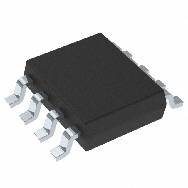
TPS2378DDA is an IEEE 802.3at Type-2 PoE PD controller in an 8-pin HSOP (PowerPAD) package. It features an internal 100 V, 0.5 Ω Hotswap MOSFET, supporting up to 0.85 A operating current with adapter priority and ESD protection.Checked against the datasheet
All alternatives
View full reportTechnical parameters
Datasheet-verified parameters
20 items| Parameter | Value and test conditions | Source |
|---|---|---|
| Package | HSOP (8) / SO PowerPAD (DDA), 4.89 mm × 3.90 mm | |
| Operating Temperature | -40 to 85 °C | |
| RoHS | Yes | |
| Recommended Input Voltage Range | RTN, VDD: 0 V to 57 V | |
| Absolute Maximum Input Voltage | VDD, DEN: -0.3 V to 100 V; RTN: -0.6 V to 100 V | |
| Recommended Junction Temperature | -40 °C to 125 °C |
All parameters (17)
| Power | |
|---|---|
| Current - Supply | 285µA |
| Number of Channels | 1 |
| Power - Max | 25.5 W |
| Voltage - Supply | 0V ~ 57V |
| Environment and package | |
| Mounting Type | Surface Mount |
| Operating Temperature | -40°C~85°C |
| Package | Tube |
| Package / Case | 8-PowerSOIC (0.154", 3.90mm Width) |
| Supplier Device Package | 8-SO PowerPad |
| Other | |
| Auxiliary Sense | Yes |
| Base Product Number | TPS2378 |
| Internal Switch(s) | Yes |
| Mfr | Texas Instruments |
| Product Status | Active |
| Series | - |
| Standards | 802.3at (PoE+), 802.3af (PoE) |
| Type | Controller (PD) |
Pinout and package
DDA Package 8-Pin HSOP Top Vie…
| Pin | Name | Function | Source |
|---|---|---|---|
| 1 | VDD: Connect to positive PoE input power rail. Bypass with 0.1 μF to VSS. | ||
| 2 | DEN: Connect 24.9 kΩ to VDD for detection. Pull to VSS disable pass MOSFET. | ||
| 3 | CLS: Connect resistor from CLS to VSS to program classification current. | ||
| 4 | VSS: Connect to negative power rail derived from PoE source. | ||
| 5 | RTN: Drain of PoE pass MOSFET. | ||
| 6 | CDB: Active low, open-drain converter disable output, referenced to RTN. | ||
| 7 | T2P: Active low indicates type 2 PSE connected or APD active. | ||
| 8 | APD: Raise 1.5 V above RTN to disable pass MOSFET and force T2P active. | ||
| Pad | Pad: The PowerPad must be connected to VSS. A large fill area is required to assist in heat dissipation. |
Documents
Datasheet-verified content is extracted by AI from the manufacturer datasheet. Click a page number to view the original.