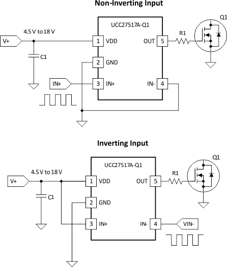

The UCC27517A-Q1 single-channel high-speed low-side gate-driver device effectively drives MOSFET and IGBT power switches. With a design that inherently minimizes shoot-through current, the UCC27517A-Q1 sources and sinks high peak-current pulses into capacitive loads offering rail-to-rail drive capability and extremely small propagation delay typically 13 ns. The UCC27517A-Q1 device handles –5 V at input. The UCC27517A-Q1 provides 4-A source and 4-A sink (symmetrical drive) peak-drive current capability at V DD = 12 V. The UCC27517A-Q1 operates over a wide V DD range of 4.5 V to 18 V and wide temperature range of –40°C to 140°C. Internal Undervoltage Lockout (UVLO) circuitry on V DD pin holds the output low outside V DD operating range. The ability to operate at low voltage levels such as below 5 V, along with best-in-class switching characteristics, is especially suited for driving emerging wide band-gap power-switching devices such as GaN power-semiconductor devices.
Все аналоги
Полный отчётТехнические параметры
| Питание | |
|---|---|
| Channel input logic | Inverting, Non-Inverting |
| Input negative voltage (V) | -5 |
| Input supply voltage (max) (V) | 18 |
| Input supply voltage (min) (V) | 4.5 |
| Number of channels | 1 |
| Peak output current (A) | 4 |
| Power switch | GaNFET, IGBT, MOSFET |
| Undervoltage lockout (typ) (V) | 4 |
| Характеристики по постоянному и переменному току | |
| Fall time (ns) | 7 |
| Propagation delay time (µs) | 0.013 |
| Rise time (ns) | 9 |
| Условия эксплуатации и корпус | |
| Operating temperature range (°C) | -40 to 125 |
| Другое | |
| Driver configuration | Inverting, Non-Inverting |
| Features | Hysteretic Logic |
| Input threshold | CMOS, TTL |
| Rating | Automotive |